3D Printed Chip Packaging Specialist XTPL Enters Japanese Market – 3DPrint.com
The additive manufacturing (AM) industry naturally wants to move beyond prototyping to production at scale, and the industry is certainly starting to demonstrate success with that objective, especially in Asia. Still, every vertical in the midst of adopting AM is in its own unique phase of technical maturity, and the path from prototyping to production looks slightly different for every application.
Additionally, every vertical that the AM industry is targeting has its own approach to R&D, and nowhere is this more apparent than with the semiconductor sector. To put things in perspective, the semiconductor sector is currently spending an estimated $150-200 billion annually on R&D, which is around 9x the size of the entire AM industry. Additionally, the revolution in chip packaging that I’ve been writing about all year is one of the most significant current drivers of semiconductor sector R&D spend, which gives companies at the intersection of AM and semiconductors an outsized opportunity to benefit.
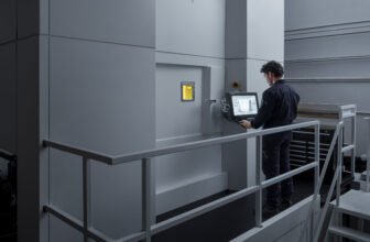
Polish original equipment manufacturer (OEM) XTPL is seizing on this opportunity, and has just announced its first sale in the Japanese market, following sales earlier this year in Taiwan and Silicon Valley. Moreover, the company’s sale of an Ultra Precise Dispensing (UPD) module to its unnamed Japanese client represents entry into a new market, and deployment of a new material offering, as well as a first foothold in a new geography.
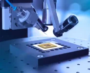
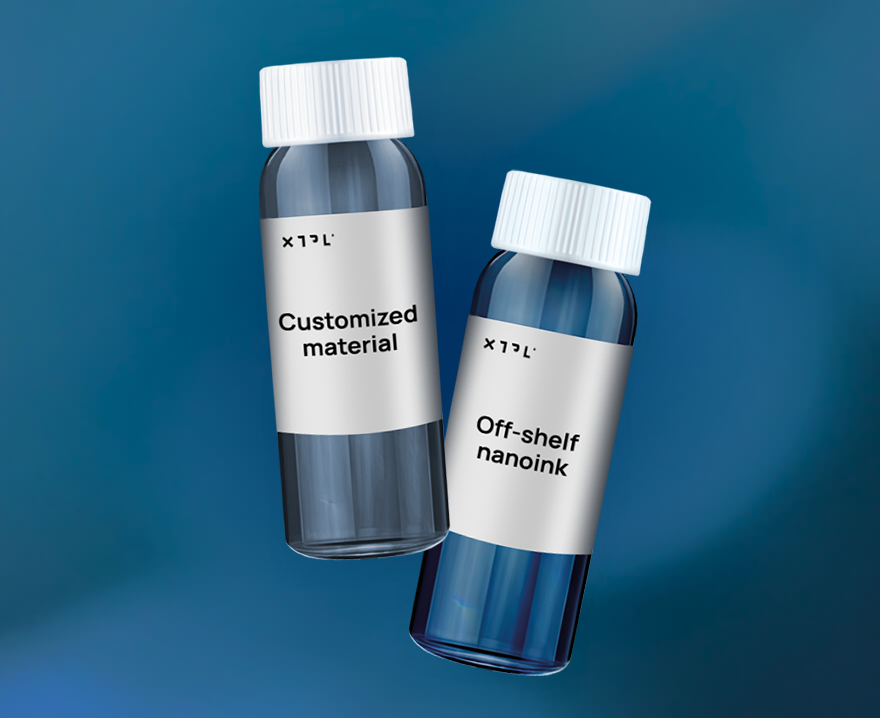
Whereas XTPL’s previous sale in Taiwan involves the flat panel display production process, the Japanese client is proving out the tech for advanced printed circuit boards (PCBs) as well as advanced packaging applications. What’s more, it’s XTPL’s first time offering copper-based materials, the most important category for the advanced packaging market.
XTPL plans to deliver the UPD module in Q4 2026, at which point the Japanese client — which, while undisclosed, is “a publicly listed…advanced automated industrial equipment manufacturer” — will install the printhead in a prototyping machine that’s currently under development. Perhaps the most notable detail is that the customer is purchasing the device specifically to test its potential for use at industrial scale.
In a press release about XTPL’s first sale to the Japanese market, the company’s CFO, Jacek Olszański, said, “The order from Japan…[is] a completely new project that immediately enters the most advanced part of our industrial pipeline. This proves that the development of UPD technology is driven not only by progressing existing projects through subsequent stages, but also on securing new, advanced engagements with global partners.
“Following the industrial implementation in the FPD segment in China, the Japanese project adds to a pool of five other XTPL projects currently at the fourth stage of evaluation, namely testing on a prototype industrial machine integrated with our UPD module. In this case, the specification is significantly more advanced, which translates into an approximately twofold higher unit value of the module compared to our Chinese deployment.”
Thus, if one were to view what XTPL is doing through a simplistic “production vs. prototyping” lens, the takeaway would be that six of XTPL’s customers currently use the company’s technology for R&D. However, if you view the company’s activity through the lens of the vertical it’s targeting, the reality emerges that XTPL is on the brink of converting six customers from prototyping to production at scale.
While the semiconductor sector is admittedly unique, the experience of the AM industry in other sectors, including defense and medical, similarly reflects the effectiveness of embedding a pathway from prototyping to production in one’s business strategy. Again, that pathway looks different for every vertical, but there are commonalities nonetheless, such as the need to execute digital transformation at an organizational level.
To narrow the focus to the semiconductor sector again: especially in the West, I think the AM industry still doesn’t realize quite how large a market opportunity chip packaging is going to be. TDK’s acquisition of Fabric8Labs should change that to some extent.
One angle explaining the deal is data center hardware, but TDK appears just as interested in Fabric8Labs due to chip packaging. Fabric8Labs may have a rather standalone manufacturing process, but there’s reason to think that, at least in China, manufacturers are exploring more widely used processes to see if they can translate to chip packaging workflow.
Images courtesy of XTPL
Subscribe to Our Email Newsletter
Stay up-to-date on all the latest news from the 3D printing industry and receive information and offers from third party vendors.
Upload your 3D Models and get them printed quickly and efficiently.